

OpenAI is preparing to launch its first custom artificial intelligence chip, marking a major shift in the company’s strategy as it seeks to reduce dependence on Nvidia and strengthen control over its own computing infrastructure. The chip, internally referred to as an “XPU,” is being co-developed with Broadcom and is
Read More
Why Combo DDR Still Matters
In today’s fast-paced SoC market, memory flexibility is no longer a luxury—it’s a competitive necessity. While DDR5 is gaining traction in high-performance systems, DDR3 and DDR4 remain dominant in embedded, industrial, and cost-sensitive markets. A combo DDR3/4 interface offers engineers a way to
SUNNYVALE, Calif., Sept. 3, 2025 — Today Synopsys (Nasdaq: SNPS) announced expanding Synopsys.ai™ Copilot generative AI (GenAI) capabilities for its industry-leading semiconductor design solutions, enabling semiconductor engineering teams to accelerate development timelines, support significantly more complex designs, and increase engineering velocity amidst a workforce shortage.
Synopsys pioneered AI as a
Read More
Woodcliff Lake, New Jersey — September 4, 2025 — Semiconductor intellectual property core provider CAST today announced that the TSN Switch IP core it offers has been integrated by RANiX Inc. in their new automotive Integrated Micro Flat Antenna System (IMFAS) system on chip (SoC).
RANiX is a global

Sept. 03, 2025 – Lawrenceville, GA — Silicon Creations, a leading provider of high-performance analog and mixed-signal IP, is proud to announce its selection as Analog Mixed Signal IP Partner of the Year by GlobalFoundries (GF). The award was presented at the GTS North America event on August 28, 2025, in Santa Clara,
Read More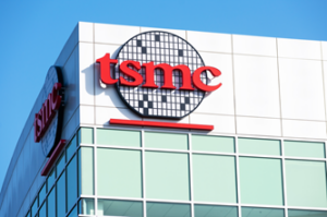
Taiwan Semiconductor Manufacturing Company (TSMC) will break ground next month on its most advanced fabrication plant to date, focused on the 1.4-nanometer process node, internally known as A14.
The new project, located in the Taichung sector of the Central Taiwan Science Park, will form part of Fab 25. This