

Automotive product traceability has existed in one form or another for several decades. Traceability generally refers to tracking and tracing each component that comprises every sub-system in a car. Traditionally, this has been achieved with direct part marking on mechanical or electronic components, using 1D or 2D barcodes or radio-frequency
Read More
PHIX B.V. of Enschede, The Netherlands, is a Dutch packaging foundry that assembles their customers’ photonic integrated circuits into complete modules. As these modules evolve from initial prototypes into mature products, the manufacturing volumes become much larger and a higher level of automation is required. This aspect of photonic device
Read More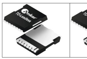
With each passing year, emerging growth application areas such as Automotive, Cloud Computing, Industrial Automation and Telecom (5G) Infrastructure are garnering more attention. Although the application segments are different, there is commonality in how voltage conversion and power distribution are achieved at the system level. System demands are becoming more
Read More
One of the most common factors that can have a lasting impact on any given semiconductor device is heat. Any logic circuit or electronic device requires a power supply to drive the function of its parts. While most of this power is used up for basic logic functions and signal
Read More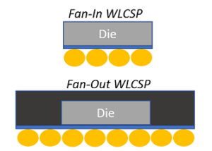
“Fan-out packaging continues to evolve, establishing a new market class, UHD Fan-Out,” asserts Favier Shoo, Technology & Market Analyst at Yole Développement (Yole). “Being actively explored and validated as one of the high performing and multi-die packaging platforms, Fan-Out Packaging is breaking through into new applications in 5G and HPC. In the Fan-Out Packaging: Technologies
Read More
WLP will definitely be a winner by 2025, declared Yole Développement (Yole) in its new Advanced Packaging Quarterly Market Monitor. $2.5B will be the market figure to remember as it will be Fan-out (FO) package revenue by 2025. Behind this data, there is TSMC’s strategy to drive fan-out for 5G applications. In parallel,
Read More