
“The demand for SiP[1] has increased significantly in recent years, with an adoption in a wide ranging of applications”, announces Favier Shoo, Technology & Market Analyst at Yole Développement (Yole). “SiP involves low-end including smaller package size & lower I/O count and high-end applications with larger package size & higher I/O. SiP is also leveraging
Read More
“Advanced packaging solutions will double their market shares within the automotive industry in the coming 5 years, reaching US$550 million” announces Mario Ibrahim, Technology & Market Analyst at Yole Développement (Yole).
Two automotive megatrends, autonomy and electrification are today pushing the development of multiple devices with dedicated packaging. Without doubts, the automotive
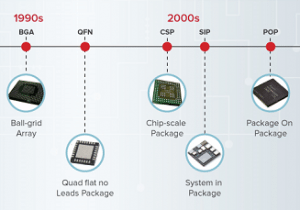
Lead Frame Overview
A lead frame is a generic term for a type of (mostly) low-cost IC package assembly used for DIL types packages as well as PLCCs and QFNs.
The frame is typically made of a thin layer of copper, though other materials, such as aluminum
Read More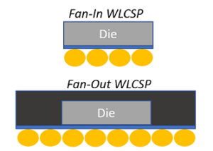
Extracted from: Equipment and Materials for Fan-Out Packaging report and Fan-Out Packaging: Technologies & Market Trends, Yole Développement, 2019
“Although the inflated excitement has started to plunge after few years of hype, Fan-Out technologies are still very well established in low-end and high-end applications”, asserts Favier Shoo, Technology & Market Analyst at Yole
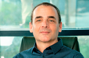
This interview was help with Mr. Oren Beckermus, which is Co-CEO of Beckermus.
Tell me about Beckermus Technologies?
Beckermus Technology is a privately-owned company, I co-own it with my brother, Oded Beckermus, the name of the company as you can already guess comes from our family

The leading giant of the OSATs, ASE Technology Holding Co., Ltd. (formerly ASE Inc.) and subsidiaries, has just got even bigger after the official acquisition of SPIL on April 30 2018. In 2018e, ASE Technology Holding Co., Ltd and subsidiaries made a new record-high revenue of US $12,308 billion, which
Read More