
Semiconductor integrated circuits (ICs) are an essential component of every other modern technology which is why they have undergone some of the most extensive growth. Today, IC packaging offering is wide and deep with many kinds and types of semiconductor packaging technologies. Your goal is, therefore, to select an IC
Read More
This interview was held with Mr. Oliver Maiwald, CEO of Sencio B.V.
Tell me a bit about your background? How did you first get started with Sencio?
I have had a fairly circuitous route to the role of CEO. My first step was as an electrical technician working on the
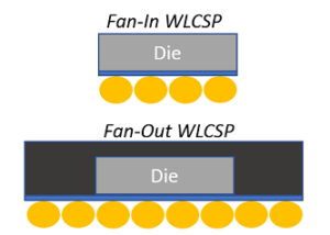
“Fan-Out Packaging is now a must-have in the portfolio to stay competitive,” asserts Favier Shoo, Technology & Market Analyst and part of the Semiconductor & Software team at Yole Développement (Yole). “New milestones are achieved by SEMCO and PTI with FOPLP technology. Both companies have invested and developed FOPLP for
Read More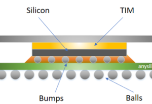
Ball Grid Array, commonly known as BGA, is one of the most widely used semiconductor package types for integrated circuits that require a high number of I/O connections, good electrical performance, reliable board mounting and efficient use of PCB area.
In a BGA package, the external connections are arranged
Amkor Technology, a leading provider of outsourced semiconductor assembly and test (OSAT) services, today announced the extension of its MEMS and Sensor package platforms to address the growing optical market. The new optical package platforms are derivatives of our successful ChipArray® BGA and MicroLeadFrame® product families and can be used for many applications including
Read More
Beckermus Technologies was founded in 1998 and serves as an Excellence Center in the field of “Bare Die” assembly services for micro-electronic and micro-optical systems. Beckermus Technologies has been playing a vital role in the lifecycle of many products, for numerous companies worldwide, from early prototypes to mass production.
Read More