

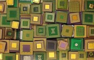
Despite the common belief, OSAT (Outsourced Semiconductor Assembly and Test) companies are very innovative. Many look at TSMC or Synopsys and consider their R&D work as innovative. But actually, semiconductor assembly industry is as innovative as any other company in the industry. We just don’t hear about it.
Semiconductor

Advanced Semiconductor Engineering, Inc. (ASE, TAIEX: 2311, NYSE: ASX), and Cadence Design Systems, Inc. (NASDAQ: CDNS), today announced they have collaborated to release a System-in-Package (SiP) EDA solution that addresses the challenges of designing and verifying Fan-Out Chip-on-Substrate (FOCoS) multi-die packages. The solution consists of the SiP-id™ (System-in-Package – intelligent
Read More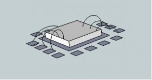
System performance is a critical requirement for the vast majority of integrated circuits that are designed today. To meet these stringent performance requirements, IC designers invest considerable time and effort in accurately modeling and simulating chip level performance – all to avoid nasty surprises when the first chips return from fabrication. Performance
Read More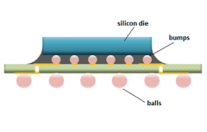
If you were uncertain about the term “FlipChip” this tutorial will help you better understand what FlipChip packaging technology is all about.
FlipChip package technology has been around for 3-4 decades and started as a package solution for high pin count & high performance package requirements. At the beginning,

Abstract
Expanding its ChipArray® Ball Grid Array (CABGA) package form factor miniaturization efforts, Amkor now offers a maximum 0.40 mm height CABGA assembly process. Amkor’s latest CABGA process has been extensively demonstrated, evaluated and optimized to provide reliable, high-quality production. By extending CABGA capabilities to various competing near die size
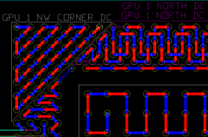
Higher bus speeds and lower power consumption are design criteria for most modern digital electronic products. Packaging solutions that provide higher bus speeds at reduced power per bit ratios require design techniques that shorten the distance between chips (to reduce drive currents) and use wider data buses (with finer line-space
Read More