


AnySilicon, the fastest-growing semiconductor vendors platform has announced today the availability of its free Semiconductor Package Price Estimator which provides package price for all major semiconductor packaging type.
Using this free tool, companies can get quick price estimation for the packaging and assembly prices which are becoming critical in many

All the work that’s been done on stacked die really could pay off soon.
The challenges of Moore’s law scaling at advanced technology nodes are well documented. I won’t repeat them here. The benefits of “more than Moore” scaling (i.e., 2.5D and 3D ICs) are also well-known. This technology
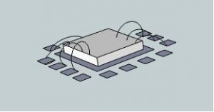
An integrated circuit package has the sole purpose of protecting and maintaining one or more integrated circuits. It is usually in the form of a plastic, glass, metal, or ceramic casing which creates a physical barrier of protection against things like impact and corrosion. Furthermore, it helps to hold contact
Read More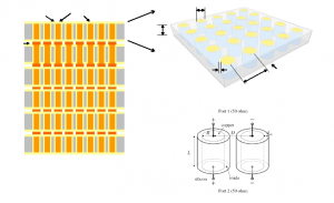
Over the last several years, the buzzword in the electronics industry has been “More than Moore”, referring to the embedding of components into the package substrate and stacking of ICs and packages using wirebond and package on package (POP) technologies. This has led to the development of technologies that can
Read More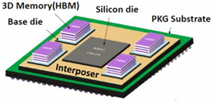
High-bandwidth memory (HBM) is a JEDEC-defined standard, dynamic random access memory (DRAM) technology that uses through-silicon vias (TSVs) to interconnect stacked DRAM die. In its first implementation, it is being integrated with a system-on-chip (SoC) logic die using 2.5D silicon interposer technology.
In June 2015, AMD introduced its Fiji
SK hynix, Inc., Amkor Technology, eSilicon, Northwest Logic and Avery Design Systems have joined forces to offer a complete high-bandwidth memory (HBM) supply chain solution. HBM is a JEDEC-defined standard that utilizes 2.5D technology to interconnect an SoC and an HBM memory stack. Many companies are already using HBM to
Read More