

Despite the rising cost for IC development, EDA tools and mask sets semiconductor design companies continue to use the most advanced CMOS technology for high performance applications because benefits like lower power dissipation, increased gate density, higher speed and lower manufacturing cost per die more than compensate the higher cost.
This return on investment however only pays off for ultra high volume applications. Due to the use of sensitive elements (such as ultra thin-oxide transistors, ultra-shallow junctions, narrow and thin metal layers), increased complexity through multiple voltage domains and the use of IP blocks from various vendors, a comprehensive ESD protection strategy becomes more important.
This white paper presents on-chip ESD protection clamps and approaches for 40/28nm CMOS that provide competitive advantage by improved yield, reduced silicon footprint and enable advanced multimedia and wireless interfaces like HDMI, USB 3.0, SATA, WiFi, GPS and Bluetooth. The solutions are validated in tens of products running in foundry and proprietary fabrication plants.
Various sources [1-3] have estimated the total development cost of a complex SoC design in 40nm somewhere between $30M and $80M, depending on the application. Due to the shrinking design rules the lithography masks get more expensive at every node now up to a few million dollars at 40nm. Further, also the cost for EDA software continues to rise because both the SoC designs and the process design constraints get more complex requiring ever more powerful software. This growing complexity is also visible in the rising labor costs for design, layout and test.
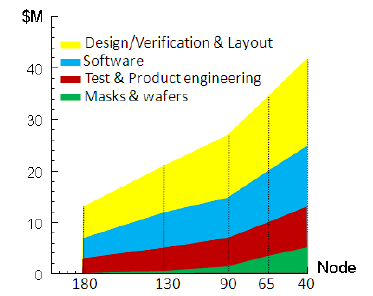
Figure 1: SoC development cost estimation, reaching more than $40M at 40nm – source International Business Strategies & Altera.
Despite this rising development cost IC design companies continue to use the most advanced CMOS technology for high performance applications because benefits like lower power dissipation, increased gate density, higher speed and lower manufacturing cost per die more than compensate the higher cost.
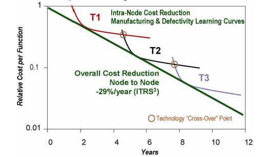
Figure 2: Relative cost per function is one of the driving forces behind the CMOS technology scaling.
Analysts believe [4] that for IC designs the return should be 10X the development cost which means that a 40nm project should present a $300M to $800M market opportunity. This return on investment however only pays off for ultra high volume applications.
Unfortunately, several factors can strongly reduce the market share and profit margins. For instance in the now dominant market of consumer electronics, the product cycles are much shorter and the price erosion stronger than a few years back which means that time to market is important. If your product is late by a few months a competing product can take over and reduce your potential sales by as much as 30% due to a reduced market share and reduced profit margin. The analyst firm International Business Strategies believes that a 1 year delay could wipe out 91% of the potential sales volume. The loss of potential sales volume is the main reason for ‘first-time-right’ design, much more important than the costs of debugging and re-spins.
One major factor is out of control of IC designers: the consumer electronics business is rapidly changing. One day a product is hot, the next day it is outdated and new features must be added to please end customers. IC designers must incorporate flexibility for late design changes, include programmability or create product IC’s that can cover a class of applications.
Another important factor is the yield of the production and assembly. DFM (Design for Manufacturability) covers various techniques to improve functional yield and reliability and is a must in advanced CMOS. One such reliability aspect is Electrostatic Discharge (ESD). According to experts it is responsible for at least 10% of all product failures in assembly. Due to the use of sensitive thin-oxide transistors, increased complexity through multiple voltage domains and the use of IP blocks from various vendors a comprehensive ESD protection strategy becomes ever more important.
This white paper presents on-chip ESD protection clamps and approaches for 40nm CMOS that provide competitive advantage by improved yield, reduced silicon footprint and enable advanced multimedia and wireless interfaces like HDMI, USB 3.0, SATA, WiFi, GPS and Bluetooth. The solutions are validated in tens of products running in foundry and proprietary fabrication plants.
The paper first describes the challenges for ESD protection in 40nm and 28nm CMOS followed by some ESD relevant trends and finally an overview of silicon validated clamps for core protection, high speed interconnects, wireless interfaces, overvoltage tolerant (3V) IOs.
Electrostatic Discharge (ESD) is the sudden discharge of a charged body and it is inevitable during the processing and assembly of electronic integrated circuits. Without the proper ESD control and on-chip ESD protection it leads to failures in the IC’s junctions, isolation oxides or metallization. To protect the chip, IC designers incorporate so-called clamp devices at IO pads, power pads (Vdd/Vss) and between power domains. The ESD device shunts the excess current to ground and limits the on-chip voltage drop below critical levels.
The first subsection below describes how this critical voltage drop has evolved for advanced CMOS and its influence on ESD design decisions. The second subsection describes how the use of tens of voltage domains in one IC (System on Chip) creates additional issues during ESD stress. Subsections 3 to 5 describe the ESD related constraints for special interfaces like cascoded MOS drivers, wireless RF IO’s and high speed interfaces.
IC designers use the so-called ‘ESD design window’ or ‘ESD design margin’ to define the electrical constraints for ESD protection clamps. The ESD clamp must act as high impedance element during normal operation which means that it should not turn-on below a certain voltage level (Minimum voltage level ‘Vmin’). During ESD conditions however, the protection cell must shunt the ESD current while clamping the voltage below a critical voltage level (Maximum voltage level ‘Vmax’). If the voltage rises above this level functional circuits will be damaged. For IO’s based on 1.8V or 2.5V transistors the ESD design margin is comparable to the margins available in 0.25um / 0.18um technology but for the core (thin oxide) devices ESD design is much more challenging.
The core power supply (Vdd) and IO signal voltage level has been reduced from 5V in 0.5um to less than 1V in 40nm / 28nm. The critical voltage level (Vmax) has decreased much stronger from more than 20V in 0.5um to below 4V for the core devices. The difference between the Vmin and Vmax level is the ESD design window. Both trends are summarized in figure 3. Clearly the design margin has been strongly reduced in advanced CMOS technology.
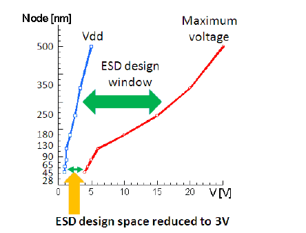
Figure 3: Shrinking ESD design margins in advanced CMOS technology. For ESD protection of 40nm / 28nm thin oxide transistors the design space is reduced to 3V seriously limiting the design choices. The ‘Maximum voltage’ is defined by the transient breakdown voltage of the core gate oxide.
While most signal interfaces in 40nm and 28nm may still use 1.8V or 2.5V IO pads IC designers have to define an ESD protection approach for the core devices too. ESD related damages can occur in the functional core of the IC’s. A few examples are given below.
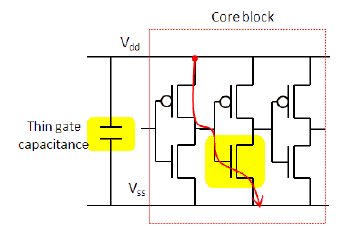
Figure 4: Core logic using thin oxide transistors reduce the maximum transient voltage at the Vdd line to about 4V: (1) the use of thin oxide gate as a decoupling capacitance (2) series connected inverters have a breakdown voltage similar to the gate oxide breakdown voltage
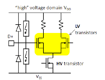
Figure 5: Analog IC designers tend to use thin oxide transistors inside thick-oxide “high” voltage domains (1.8V, 2.5V) to speed up certain analog blocks. This strongly reduces the ESD design margin in the 1.8V, 2.5V domains.
The small design margin for the core devices actually forces IC designers to take new and unique ESD protection measures because the traditional approaches have run out of steam from 90nm and 65nm nodes on. The third section provides information about silicon and product proven protection approaches for TSMC’s 40nm technology. However, besides the cases defined above other issues arise in advanced CMOS circuits. The next subsections describe additional considerations. Despite the improved ESD awareness and control in assembly factories and the related push for a reduction of component level ESD performance ICs still need adequate ESD protection.
While ESD protection has always been dealt with at the IO and power pads, many publications in the last years report ESD failures in core devices located at the ‘functional edge’ of power domains. A similar problem occurs through the use of multiple IP blocks sourced from different vendors as graphically explained in figure 6. While both IP blocks may have been tested and approved for ESD by the IP vendors or even in previous ASIC designs (‘A’ case in figure 6), the combination of the two blocks on the same chip (‘B’ case) may still lead to low ESD performance. The (‘C’) figure represents a possible implementation of such a communication line. If the voltage drop through the intended ESD protection path is too high then the receiver (IP block #2) may get damaged.
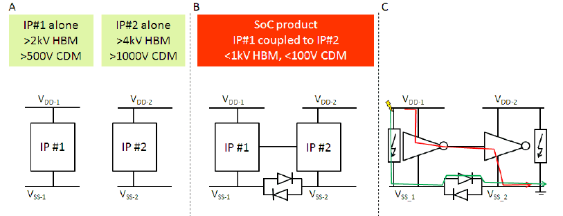
Figure 6: While each functional IP block may be tested and approved for ESD (‘A’) the combination may still create ESD issues (‘B’). ‘C’ depicts a typical scenario where a buffer in a first domain drives a distant receiver in a second supply domain: The voltage drop across the intended ESD path (green) is higher than the gate oxide breakdown of the receiver block in the second IP block. Effective core protection strategy is required to protect sensitive core devices.
System on Chip circuits in advanced CMOS typical use a multitude of power domains, each designed for certain functionality. ESD designers need to carefully investigate communication lines between different voltage domains to prevent oxide ruptures inside the core of the chip.
Another typical issue in advanced CMOS circuits is the over voltage requirement for circuits connected to older ICs. Various interfaces including for instance USB, HDMI still use so-called ‘legacy’ 3.3V or even 5V signals and supply levels. Compatibility to these voltage levels is not included in the standard CMOS process offering from the foundries and circuits must be custom developed. Designers typically use a series connection of low voltage transistors to enable communication at higher voltage levels. It takes some analog design expertise to ensure that the voltage across all terminals never exceeds the maximum ratings. Such custom designed circuits are typically very weak during ESD stress which means that dedicated local ESD protection clamps are required as the ‘dual diode’ approach cannot be used.
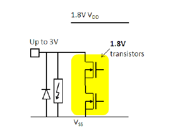
Figure 7: For compatibility with other/older ICs on the PCB board, IC designers frequently need to create custom circuits running at voltage levels beyond the capabilities of the process technology. A typical approach is to use a so-called cascode design of transistors. This represents an ESD issue as most cascode designs are sensitive during ESD stress.
The number of wireless enabled systems is very diverse and growing steadily. System makers include wireless functions into mature applications like fixed-line telephones and TV’s, increase the wireless features in mobile phones with support of multiple standards and come up with new device types that thrive on being always wirelessly connected for the newest content. Further, also the transport, security, medical and payment sectors are quickly switching to wireless interfaces for improved user experience.
Various approaches exist to protect the wireless interfaces against ESD stress. In recent years, researchers have focused on so-called ‘co-design’ techniques to solve both functional and protection constraints which requires both RF and ESD design skills. However many IC designers still prefer to work with ‘plug-n-play’ protection concepts where the ESD clamps exhibit low parasitic capacitance, low series resistance and low leakage. In many cases, traditional ESD protection devices used for low speed digital interfaces offered by foundries, IO library providers are not suited for the RF interfaces for a number of reasons:
Advanced multimedia features require high bandwidth interfaces to quickly transport video and audio content between memory and processing units. Similar to the wireless interfaces the standard IOs provided by library providers or foundries are not suited for such high speed connections due to large capacitance loading. Moreover the leakage, introduced by the large size ESD protection clamps, drastically reduces the battery time of mobile appliances.
Clearly, the use of advanced CMOS technology has introduced new challenges for ESD protection clamps. Many of these challenges cannot be solved by traditional solutions such as the ggNMOS device or LVTSCR clamps. The next section provides a brief introduction into ESD relevant trends in advanced CMOS technology. The third section provides information about silicon validated ESD clamps for TSMC 40nm CMOS coping with the different challenges discussed above.
Throughout its 10 years of existence (2000-2010) Sofics engineers have analyzed ESD protection devices across various foundries, technology nodes, voltage domains and process options. This section summarizes some of the ESD relevant trends.
Similar to other researchers [5] Sofics engineers believe that metallization of the ESD structures is becoming one of the main constraints. The metal thickness is strongly reduced during the downscaling in CMOS technology. The M1 and M2 thickness decreased with about 50% from 130nm to 40nm which strongly influences ESD performance due to increased resistivity and decreased ESD robustness levels. Similarly the contact and via design rules have led to a strong reduction of the maximum ESD current through a single contact/via (figure 8).
Another important aspect is the investigation of MOS transistors under ESD relevant conditions. Different measurement conditions are applied to study all the parameters summarized in Figure 9.
IC designers use a broad spectrum of on-chip ESD device concepts for the protection of interfaces in advanced CMOS. The trends for the robustness per area (failure current It2 per um² device area) for the main building blocks (snapback MOS, diodes and Silicon Controlled Rectifiers) are plotted on figure 10. The variation between fabs, device layouts is larger than the variation between technology nodes.
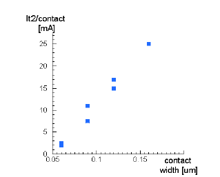
Figure 8: Failure current It2 per contact as a function of the contact width.
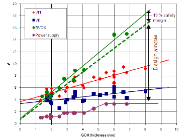
Figure 9: Summary of the measured oxide breakdown voltage (BVOX), NMOS trigger (Vt1), NMOS holding voltage (Vh) and supply voltage (Power supply) in function of the gate oxide thickness.
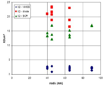
Figure 10: Overview of the ESD robustness per area for ggNMOS, SCR and diodes across technology nodes.
The following tables provide an overview of the Sofics ESD clamps for the 40nm technology for the 0.9V, 1.1V, 1.2V, 1.8V and 3.3V domains. The cells are designed for 2.5kV HBM and 200V MM (unless otherwise mentioned) but can be easily adapted for other ESD protection levels. The cells can be further customized to ensure compatibility with specific metal schemes and IO pitch.
The Sofics ESD cells cover all types of protection concepts and approaches as detailed in the figure below.
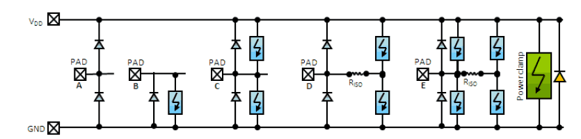
Figure 11: Different pad types available in the 40nm solution set from Sofics. For each power domain (0.9V, 1.2V, 1.8V and 3.3V) a power clamp is available. Protection cells for RF interfaces are available for the 1.1V domain. For the IO’s several pad-types exist: Pad-type ‘A’ consists of a standard dual diode. Pad-type ‘B’ is used for some RF interfaces. Pad-type ‘C’ consists of a full local protection with 2 clamps and dual diode. Pad-type ‘D’ uses dual diode as a primary protection and a secondary protection concept with small local clamps. Pad-type ‘E’ uses a full local protection concept as primary protection but adds secondary local clamps specifically for improved CDM protection levels.
| Voltage | Clamp type | Silicon | Leakage | Junction | ESD | Vt1* | Comment |
| domain | footprint | capacitance | performance | ||||
| 0.9V | Power clamp | <1000um² | <200pA | >2kV HBM | 2.36V | ||
| >200V MM | |||||||
| 0.9V | PAD-type A | <500um² | <100pA | <100fF | >2kV HBM | D | Dual diode protection not |
| >200V MM | always feasible | ||||||
| 0.9V | PAD-type C | <1500um² | <150pA | <200fF | >2kV HBM | 1.98V | Protects thin oxide output |
| >200V MM | drivers | ||||||
| 0.9V | PAD-type E | <2100um² | <100nA | <400fF | >2kV HBM | 2.36V | Protects thin oxide |
| >200V MM | bidirectional interfaces, | ||||||
| Riso=20 Ohm | |||||||
| 0.9V | PAD-type B | <1000um² | <10pA | <180fF | >5kV HBM | D | Protects thin oxide |
| >250V MM | bidirectional interfaces | ||||||
| Voltage | Clamp type | Silicon | Leakage | Junction | ESD | Vt1* | Comment |
| domain | footprint | capacitance | performance | ||||
| 1.1V | PAD-type A | <500um² | <100pA | <100fF | >2kV HBM | D | Dual diode protection not |
| >200V MM | always feasible | ||||||
| 1.1V | PAD-type B | <1000um² | <10pA | <180fF | >5kV HBM | D | Protects thin oxide |
| >250V MM | bidirectional interfaces | ||||||
| Q-factor 71 | |||||||
| 1.1V | PAD-type B | <1400um² | <100pA | <180fF | >4.5kV HBM | 3.03V | Protects thin oxide |
| >200V MM | bidirectional interfaces | ||||||
| OVT protection | |||||||
| Q-factor 43 |
| Voltage | Clamp type | Silicon | Leakage | Junction | ESD | Vt1* | Comment |
| domain | footprint | capacitance | performance | ||||
| 1.2V | Power clamp | <1000um² | <100pA | >2kV HBM | 2.8V | ||
| >200V MM | |||||||
| 1.2V | PAD-type A | <500um² | <100pA | <100fF | >2kV HBM | D | Dual diode protection not |
| >200V MM | always feasible | ||||||
| 1.2V | PAD-type C | <1700um² | <150pA | <350fF | >2.5kV HBM | 2.35V | Protects thin oxide output |
| >220V MM | drivers | ||||||
| 1.2V | PAD-type E | <2200um² | <100nA | <500fF | >3.5kV HBM | 2.99V | Protects thin oxide |
| >300V M | bidirectional interfaces, | ||||||
| Riso=20 Ohm | |||||||
| 1.2V | PAD-type E | <1900um² | <10nA | <250fF | >2kV HBM | D | Protects thin oxide |
| >200V MM | bidirectional interfaces, | ||||||
| Riso=5 Ohm | |||||||
| 1.2V | PAD-type B | <1000um² | <10pA | <180fF | >5kV HBM | D | Protects thin oxide |
| >250V MM | bidirectional interfaces | ||||||
| Voltage | Clamp type | Silicon | Leakage | Junction | ESD | Vt1* | Comment |
| domain | footprint | capacitance | performance | ||||
| 1.8V | Power clamp | <1300um² | <150pA | >3kV HBM | 3.72V | ||
| >240V MM | |||||||
| 1.8V | PAD-type A | <500um² | <100pA | <100fF | >2kV HBM | D | Dual diode protection not |
| >200V MM | always feasible | ||||||
| 1.8V | PAD-type C | <2000um² | <200pA | <400fF | >2kV HBM | 3.55V | Protects thick oxide |
| >200V MM | output drivers | ||||||
| 1.8V | PAD-type C | <1500um² | <1nA | <250fF | >3kV HBM | 2.78V | Protects bidirectional |
| >250V MM | interfaces | ||||||
| 1.8V | PAD-type E | <1900um² | <10nA | <250fF | >2kV HBM | D | Protects bidirectional |
| >200V MM | interfaces, Riso=5 Ohm | ||||||
| 1.8V | PAD-type B | <1300um² | <100pA | <100fF | >2kV HBM | 4.05V | Used as clamp for XTAL |
| >200V MM | oscillator module | ||||||
| 1.8V | PAD-type B | <1000um² | <10pA | <180fF | >5kV HBM | D | Protects thick oxide |
| >250V MM | bidirectional interfaces | ||||||
| Voltage | Clamp type | Silicon | Leakage | Junction | ESD | Vt1* | Comment |
| domain | footprint | capacitance | performance | ||||
| 3.3V | Power clamp | <2000um² | >4kV HBM | 5.7V | |||
| >300V MM | |||||||
| 3.3V | PAD-type A | <500um² | <100pA | <100fF | >2kV HBM | D | Dual diode protection not |
| >200V MM | always feasible | ||||||
| 3.3V | PAD-type B | <2000um² | >4kV HBM | 5.7V | |||
| >300V MM | |||||||
| 3.3V | PAD-type B | <1000um² | <10pA | <180fF | >5kV HBM | D | Protects thick oxide |
| >250V MM | bidirectional interfaces |
Remarks
IC design companies continue to use the most advanced CMOS technology for high performance applications because benefits like lower power dissipation, increased gate density, higher speed and lower manufacturing cost per die more than compensate the higher cost. Due to the use of sensitive thin-oxide transistors, increased complexity through multiple voltage domains and the use of IP blocks from various vendors, a comprehensive ESD protection strategy becomes more important.
This white paper presents on-chip ESD protection clamps and approaches for 40nm CMOS that provide competitive advantage by improved yield, reduced silicon footprint and enable advanced multimedia and wireless interfaces like HDMI, USB 3.0, SATA, WiFi, GPS and Bluetooth. The presented solutions are validated in more than 20 product ICs running in foundry and proprietary fabrication plants (Status December 2010).
References
__________________________________________________________
This is a guest post by Sofics, the world leader in on-chip ESD protection.


