

In the field of semiconductor design, memory compilers are software tools used to automate the process of designing and generating memory circuits for use in integrated circuits (ICs). These memory circuits can include static random access memory (SRAM), read-only memory (ROM), and dynamic random access memory (DRAM), among others.
Memory compilers work by taking input parameters such as memory size, speed, power consumption, and timing constraints and generating a memory circuit layout that meets these specifications. This automated process saves time and resources compared to manually designing memory circuits, and also helps ensure consistency and reliability across different memory designs.
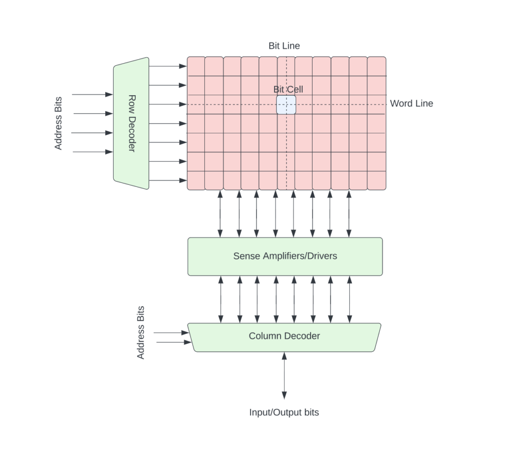
Modern SoCs and ASICs contain a plethora of memory devices like the registers and latches that can store data and support basic operations like reading from and writing to them. With the growing size of the SoCs and the need to provide more throughput, the size of the buses has increased manifold and there is a need to get bigger and faster storage space. While registers are fastest to access, they offer low packing density. For bigger storage elements, using registers (also known as Register Files) tends to be prohibitively expensive and the alternate is an SRAM. SRAMs offer higher packing density at the expense of longer access times. The size of SRAMs needed may be different for different logical elements in a design. For a chip as big as a CPU or a GPU, there may be 100-200 unique SRAM instances needed and as one might imagine, it is impossible to design these SRAMs manually.
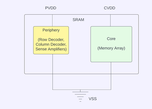
SRAM is split into two major sub-blocks:
Memory Periphery – This usually operates at the same voltage as the standard cell supply outside the memory and includes row decoders, column decoders, sense amplifiers etc.
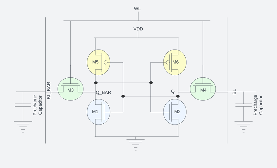
The bit cell of an SRAM is worthy of some detailed explanation. The most commonly used SRAM bit cell is the 6-T cell that comprises of 6 transistors. Transistors M1, M2, M5, M6 are the cross-coupled inverters and represent the memory element of the SRAM. Transistors M3, M4 represent the access transistors that come in play during the read or write operation and help access the memory elements when the Word line (WL) is held at logic 1. When WL is held at logic 0, the SRAM holds its value. The bit lines (BL) act as the input when we are writing into the memory, and act as an output when we are reading from the memory.
Memory Compiler offers an automated method to generate custom SRAM instances based on various input parameters like the number of words, number of bits, periphery threshold voltage, column mux ratio, number of banks etc. that is optimized for area and power. We will talk about these parameters in detail.
Speed versus Density- Some memory compilers are optimized for speed, while some are optimized for area. For SRAMs that take up significant area, going with the HD (High-Density) compiler is preferred owing to the area savings one might get. The HD memories tend to have quite large access times and may therefore limit the performance of the design. In contrast, the HS (High-Speed) compiler is optimized for the small access time, however, it comes with an area cost. HS memories are therefore preferred for smaller SRAM cuts or the ones that lie in the critical paths of the design.
Architecture: Following are the commonly used memory compilers based on the architectural specification:
The functional or the size of the memory is specified in the form of number of words.
Bits per word specify the number of bits per word in a given functional specification of the SRAM. It is worth nothing that the number of words and number of bits per word are only the functional specification. Physically, any SRAM is arranged in the form of rows and columns.
VT type specifies the threshold voltage of the transistors used to implement a given memory. This should be:
HVT: High VT offering slower access time and low leakage.
LVT: Low VT offering faster access time and high leakage.
Ultra-LVT: Very low VT offering fastest access time at the cost of very high leakage.
MVT: Mixed VT offering the right balance between access times and the leakage power.
Some compilers also support the option of more than 1 banks (bit array banks) that allows the maximum capacity of the compiled SRAM to effectively increase. Multi-bank memories use symmetrical placement of the banks to share the peripheral circuitry in such a way that the access times to any individual bank is uniform. Multi-bank memories are more area efficient as multiple banks share the same circuitry. In addition to the area, multi-bank memories also provide the option to put the individual banks into a lower power mode to conserve leakage power.
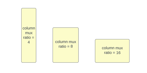
Designers are given the option to control the aspect ratio of the physical SRAM that works well for their floorplan. This is accomplished with the help of “column mux ratio”, where a lower value of column mux ratio results in taller memories while a higher value results in flatter memories.
Dual Supply Rail: Some compilers support the option of dual rail SRAMs, where the periphery of the SRAM can operate at a different power supply in contrast to the core of the SRAM.
Row Redundancy and Column Redundancy: This option means presence of spare rows and columns in the SRAM to allow replacing a faulty row or column in the fabricated SRAM with the redundant rows or columns to improve product yield. This option is sometimes also used to replace leaky cells to reduce the leakage power.
Bit Write Mask: This option allows the user to mask one or more bits when writing data to the SRAM.
Built-In Self Test and Repair (BIST/R): This option adds the support for built-in self test and repair capability to improve the product reliability and overall yield.
Power dissipation is quite a big concern, and memory compilers support following low power modes:
Nap: SRAM is said to be in nap state when the periphery supply is turned off while the core supply is still on. This mode helps conserve leakage power.
Retention: This option saves the memory states in a low power mode when the SRAM is in the power down enable mode. This mode is similar to that of a state retention power gating. In this mode, the core voltage is maintained at a minimum voltage value to retain the data.
Shutdown: In the shutdown mode, both the periphery supply and the core supply are switched off. The contents of the SRAM are lost, and this state has the lowest leakage power consumption. Since both the supplies are switched off, waking up from this state takes the longest (wake up time).
Memory compiler outputs the following files to be used downstream by physical design and other flows:
Netlist: Memory Compiler generates a netlist of the generated memory that is read by the physical design tools and needed while running the Layout versus Schematic (LVS) check and also needed during functional verification of the design.
Layout Extraction Format (LEF): This is the layout model of the SRAM used for physical placement and during extraction.
Timing Models: These are the liberty files that contains all the timing information for synthesis, static timing analysis (STA) and gate level simulations (GLS). Based on all the scenarios enabled while running memory compiler, it generates a .lib for each requested scenario.
Schematic: This is again needed for the LVS check.
Symbol: This is needed for schematic capture.
Memory Datasheet: This offers an easy-to-read summary of the key timing and area numbers of the memory across multiple scenarios.
AVM Models: AVM models are required by the EM/IR tool to perform power integrity signoff checks like static IR drop, dynamic IR drop etc. These files contain the current numbers for every mode like the read or write or read/write, leakage current numbers, the decoupling capacitance numbers, the SDF conditions and the output load assumed for each output pin. EM/IR tools use this information to deduce the current waveform at the SRAM power pins to subsequently use them for voltage drop analysis.
The vendors usually provide a different memory compiler binary for different technologies like FINFET or FDSOI or CMOS, for different technology nodes and different foundry partners.


