
Get the semiconductor daily news directly to you by subscribing to our email list. For ASIC designer and managers, staying updated with the latest news, technologies, and trends is crucial. Here are the lastest news from the semiconductor industry.

Rising design complexity is leading to near exponential increase in verification efforts. The industry has embraced verification reuse by adopting UVM, deploying VIPs and plugging block level env components at sub system or SoC level. According to a verification study conducted by Wilson research in 2012 (commissioned by Mentor) the engineers spend ~60%
Read More
Companies are using FPGAs for the variety of benefits they offer, including:
Rapid-prototyping
Running large sets of test data
Software development
The advantages of using FPGAs for verification include:
Smaller, less complex designs can be verified solely by building them in an FPGA
Read More

IC Insights has raised its worldwide IC market growth forecast for 2017 to 11%—more than twice its original 5% outlook—based on data shown in the March Update to the 20th anniversary 2017 edition of The McClean Report. The revision was necessary due to a substantial upgrade to the 2017 growth
Read More
AnySilicon is proud and exited to launch our first quiz series.
[wp_quiz id=”4859″]

The integrated circuit, sometimes called a ASIC, IC, or just a chip, is a series of transistors placed on a small, flat piece that is usually made of silicon. The IC is really a platform for small transistors that a small chip which can operate faster than old-fashioned large transistors
Read More
The IC industry’s original system-on-chip (SoC) product category—microcontrollers—is expected to steadily reach record-high annual revenues through the second half of this decade despite an overall slowdown in unit growth during the next five years. Microcontroller sales barely increased in 2015, rising less than a half percent, to set a
Read More
he increasing value of the average IC content in cellular handsets along with the increasing percentage of smartphones sold as a percent of total cellular handsets will help drive the cellphone IC market to $94.3 billion in 2019. Strong double-digit growth rates in the cellular handset IC market were
Read More
Total yearly semiconductor unit shipments (integrated circuits and opto-sensor-discrete, or O-S-D, devices) are forecast to continue their upward march and are now expected to top one trillion units for the first time in 2018, according to data presented in IC Insights’ recently released 2016 edition of The McClean Report—A
Read More
In the February 22-28 issue of Bloomberg Businessweek magazine, Johny Srouji, Apple’s senior vice president for hardware technologies, discusses Apple’s winning strategy of owning its own silicon. http://www.bloomberg.com/features/2016-johny-srouji-apple-chief-chipmaker/ . It began with the acquisition a Silicon Valley chip startup called P.A. Semi in April of 2008 and since then, Apple
Read More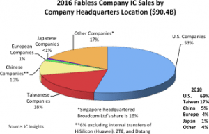
Research information that will be posted in the March Update to the 20th anniversary 2017 edition of IC Insights’ McClean Report shows that fabless IC suppliers represented 30% of the world’s IC sales in 2016 (up from only 18% ten years earlier in 2006). As the name implies, fabless IC
Read More