

Clock is the heart of synchronous digital systems. All the events in an SoC are controlled by the active edge of the clock and clock frequency is often synonymous with throughput and performance. The distribution of clock is an interesting problem involving a plethora of design trade-offs. Designers need to understand the trade-offs and choose a distribution methodology that meets all their design goals. In this post, we will discuss some of the metrics that help qualify the clock tree, and also discuss 3 most commonly used clock tree distribution methodologies.
Some of the metrics that help qualify the clock tree are:
Clock skew refers to the difference in arrival times of the clock signals at the sequential elements in the SoC design.
Positive Clock Skew means that the clock arrives at the capturing sequential later than it arrives at the launching sequential. This scenario aids setup timing, while making hold timing more critical.
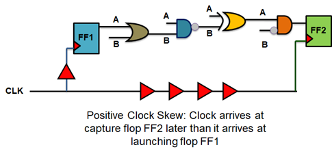
Figure 1: Positive Clock Skew
Negative Clock Skew means that the clock arrives at the launching sequential later than it arrives at the capturing sequential. This scenario aids hold timing, while making setup timing more critical.
Another skew metric that SoC designers are usually concerned with is the local clock skew and the global clock skew.
Local Clock Skew refers to the clock skew between any two sequentials with a valid timing path between them. Local clock skew directly impacts timing.
Global Clock Skew refers to the clock skew between any two sequentials in the design irrespective of whether a timing paths exists between them. While global skew doesn’t impact timing, it gives an idea of how well the clock is distributed across the design.
Clock routing takes up significant amount of chip routing resources. Clock needs to compete with power to take up top metal layers to facilitate faster and a balanced clock distribution. For highly utilized designs, signal routing resources usually come at a premium. Clock signal may also be routing using NDRs (Non-Default Routing) rules, allowing designers to route clock signals using non-default width and/or non-default wire spacing.
Another factor that designers need to gauge is the need for shielding the clock signals. Clock signal being the highest frequency signal in the design, acts as an aggressor to induce noise into the signal nets in the vicinity. In order to mitigate this noise, designers like to shield their clock signals with power/ground signals, thereby further decreasing the number of available routing resources for the signal nets.
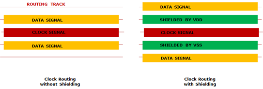
Figure 2: Clock Shielding
The clock frequency specification and the standard cell utilization target motivates designers to choose a particular clock tree distribution.
Clock power may account for more than 50% of the total power dissipated in the design. The choice for clock architecture will have an impact on total power dissipated in the design. Major clock power components are as follows:
Dynamic Power– Dynamic power is the power dissipated in the clock network while the clock network is switching. Clock signal toggles twice every clock cycle and unless gated, toggles incessantly. Dynamic power is a function of clock frequency, the switching factor, the operating voltage and the clock net capacitance.
![]()
Internal Power– Internal power is the power dissipated due to the flow of crow-bar current from the power rail to the ground node while both the pull-up and the pull-down network of the clock cells are ON. Internal power directly depends on the clock slew. Worse clock slew allows more crow-bar current and therefore increases the internal power dissipated.
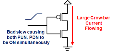
Figure 3: Internal Power
OCVs refer to intra-chip variations in Process, Voltage and Temperature which may result in delay variations of standard cells on silicon. With shrinking technology nodes, the impact of On-Chip Variations has been ever increasing. Clock path to launch and the capture sequential needs to diverge at some point along the clock network. Any clock cells in the clock network before the point of divergence are immune to any OCV variations, while the clock cells after point of divergence are susceptible to intra-chip variations, and may exhibit different delay on silicon. Designers need to model this OCV variation in form of clock skew. Depending upon the clock architecture chosen, the point of divergence may be upstream or downstream along the clock tree.
Designers may need to choose from among 3 clock distribution methodologies depending on their design specifications:
Clock Tree Mesh
As the name suggests, clock tree mesh involves a dense mesh of shorted wires to distribute the clock to every corner of the design. It involves many mesh drivers driving a capacitive mesh of wires which are shorted to effectively ensure that the clock arrives at the same time along all points on the mesh. If the mesh is dense enough, it only requires a few stages of clock network (2-3 stages) to route the clock to the sequentials in the design. This ensures that the point of divergence is downstream into the clock network, and therefore helps achieve minimum impact of OCVs. Also, the clock skew tends to be minimum.
The downside of using a clock mesh is that any clock gates are usually connected after the mesh, thereby implying that the entire mesh is always ON and switching continuously. Clock mesh designs are therefore expensive on power dissipation and routing resources.
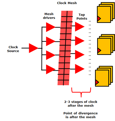
Figure 4: Clock Tree Mesh
Single Point CTS
Single point CTS lies on other extreme of the clock tree architectures where point of divergence lies at the clock source. This allows clock gates to be inserted strategically at the source to allow clock to be gated in order to save dynamic power. Also, this architecture would be judicious on the usage of clock routing resources. On the downside, single point CTS is most susceptible to impact of OCVs and may result in pretty large clock skew.
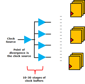
Figure 5: Single Point CTS
Multi-Source CTS
Multi-source CTS is a trade-off between clock tree mesh and single point CTS in terms of all the metrics discussed above. It involves a global distribution network in form of a sparse mesh or an H-tree with tap points strategically inserted at different locations. These tap points are followed by a local clock tree distribution to route clock from these tap points to the clock end-pins. MS-CTS offers lower power dissipation with respect to clock tree mesh, but a better skew in contrast to single point CTS.
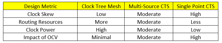
Table 1: Comparison of different clock architectures on various design metrics
Clock tree distribution is a critical design decision that involves many trade-offs for power, performance and routing resources. Designers need to understand their requirements and the architectural specifications to choose the clock distribution architecture that meets their goals.


