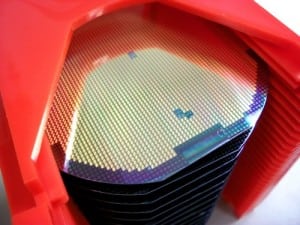
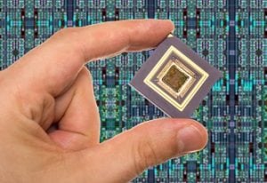
Gallium arsenide (GaAs) technology is a type of semiconductor material used in the manufacturing of various electronic devices. It is known for its high electron mobility, which allows it to operate at higher speeds and with lower power consumption compared to other semiconductor materials such as silicon. GaAs technology is ...
PHIX B.V. of Enschede, The Netherlands, is a Dutch packaging foundry that assembles their customers’ photonic integrated circuits into complete modules. As these modules evolve from initial prototypes into mature products, the manufacturing volumes become much larger and a higher level of automation is required. This aspect of photonic device ...
When a semiconductor device fails, the visible damage is not necessarily the root cause. A damaged metal line, cracked package, leaking transistor or burned bond wire may be the final result of a sequence of events rather than the original problem. The purpose of the semiconductor failure analysis process is therefore to ...
Scanning Electron Microscopy (SEM) is one of the most important imaging techniques used in semiconductor failure analysis. While optical microscopes remain extremely useful for initial inspection, many semiconductor defects are simply too small to characterize adequately with visible-light microscopy. SEM uses a focused beam of electrons rather than light, allowing engineers ...
OBIRCH (Optical Beam Induced Resistance Change) is a laser-based fault-localization technique used in semiconductor failure analysis to identify electrically abnormal regions such as resistive shorts, leakage paths, defective vias and interconnect problems.
The technique works by scanning a focused laser across an electrically biased semiconductor device. Local laser heating changes the ...
Creonic’s DVB-S2 and DVB-S2X IP cores now include support for the new DVB-NIP standard on physical layer — an important step toward seamless integration of satellite and IP-based network technologies.
The DVB-NIP standard is designed to facilitate the native transport of IP over satellite networks, extending the capabilities of DVB-S2X by streamlining packet-based data delivery.
With ...
Hsinchu, Taiwan -- July 11, 2023 -- Faraday Technology Corporation (TWSE: 3035), a leading ASIC design service and IP provider, launched its SerDes (serializer/deserializer) total solution comprises SerDes IP design on UMC 28nm and the corresponding IP advanced (IPA) service which includes IP subsystem integration, PHY hardcore implementation, and signal integrity/power ...
Kaiserslautern, Germany – July 31, 2025 – Creonic GmbH, the leading provider of cutting-edge communications IP cores, announces the release of Version 6.0 of its DVB-S2X Demodulator IP core. This major update introduces powerful enhancements that expand the configurability and technical performance of one of Creonic’s most mature and widely ...
With the creeping rise in the price of gold, many microelectronics manufacturing companies have been looking for alternatives to reduce the cost of ball bonding. Recently, the trend has been to look into the use copper wire. However, there are many drawbacks to using copper wire, including the short shelf ...
Hsinchu, Taiwan -- June 24, 2025 -- Faraday Technology Corporation (TWSE: 3035), a leading ASIC design service and IP provider, today announced the availability of its 10G SerDes IP on UMC’s 22nm process technology. Designed to meet the increasing demands of high-speed data transmission, the new SerDes IP supports a broad ...