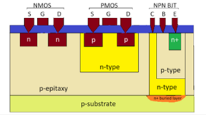
The richest directory of ASIC/IC FIB services worldwide. Find the IC FIB services companies that matches your needs.
37 results found See AllSend Email to All
The factors affecting silicon wafer cost are numerous. From the resistivity required for different applications to the physical size of the wafers, and not least the quality grades that separate the pristine from the less perfect; each aspect intricately influences the cost. As we embark on this explanation, we'll unwrap the ...
The Qmode project is funded with an MIT-R&D collaboration project grant from the Provincie Overijssel, dedicated to stimulate the innovation and development of products, processes and services of local SMEs working in the Dutch Top Sectors. The collaboration established in Qmode will help QuiX secure a leading position in the ...
Chiplets are a relatively recent advancement in semiconductor technology that involves breaking down a traditional monolithic integrated circuit (IC) into smaller, individual semiconductor components or "chiplets." These chiplets can be designed and manufactured independently, and then they are integrated onto a common substrate or package to create a more complex ...
Getting funding for a semiconductor startup is not getting easier. According to CBIngishts, there have been fewer than 20 Angel/Seed and Series A deals in the USA in each year since 2009. So where is all the funding channeled to? In 2013, close to a quarter of all VC funding was ...
Introduction to Semiconductor Semiconductors have a small energy gap between the conduction and valance bands, and their conductivity is between insulators and conductors. At absolute zero temperature, semiconductor materials are pure insulators and gradually increase with temperature. Temperature and doping are the two mechanisms to manage the conductivity of semiconductors. Doping ...
Silicon Valley, CA (Feb 9, 2021) - Integra Technologies, a world leader in semiconductor packaging, assembly, test, characterization and related services, today announced the successful implementation of a high accuracy fiber array waveguide attachment system focused on the Silicon Photonics market. This latest set of tools is based on the double-sided HexNano ...
UK
NanoScope is a European Focused Ion Beam Technology and TEM Microscopy service provider.
Failure Analysis, Circuit Nano-edit, Reliability Testing, FIBxTEM Analysis
View vendor pageOverview of Silicon-Germanium (SiGe) Technology and Historical Development Shockley's early transistor game most likely inspired the notion of fusing silicon (Si) and germanium (Ge) to create an alloy for use in transistor engineering. However, this concept has just become a reality in the last 15 years due to the challenges associated ...
Gallium arsenide (GaAs) technology is a type of semiconductor material used in the manufacturing of various electronic devices. It is known for its high electron mobility, which allows it to operate at higher speeds and with lower power consumption compared to other semiconductor materials such as silicon. GaAs technology is ...
One of the leading manufacturers of automatic test equipment, Advantest has proven to be one of the leading lights in the semiconductor industry. In addition, they manufacture measuring instruments that are used in the creation of electronic system. You can find Advantest products used in the creation of digital consumer ...
Try our free service and get free vendor
quotes, while remaining anonymous.
No thanks. Let me keep searching.